

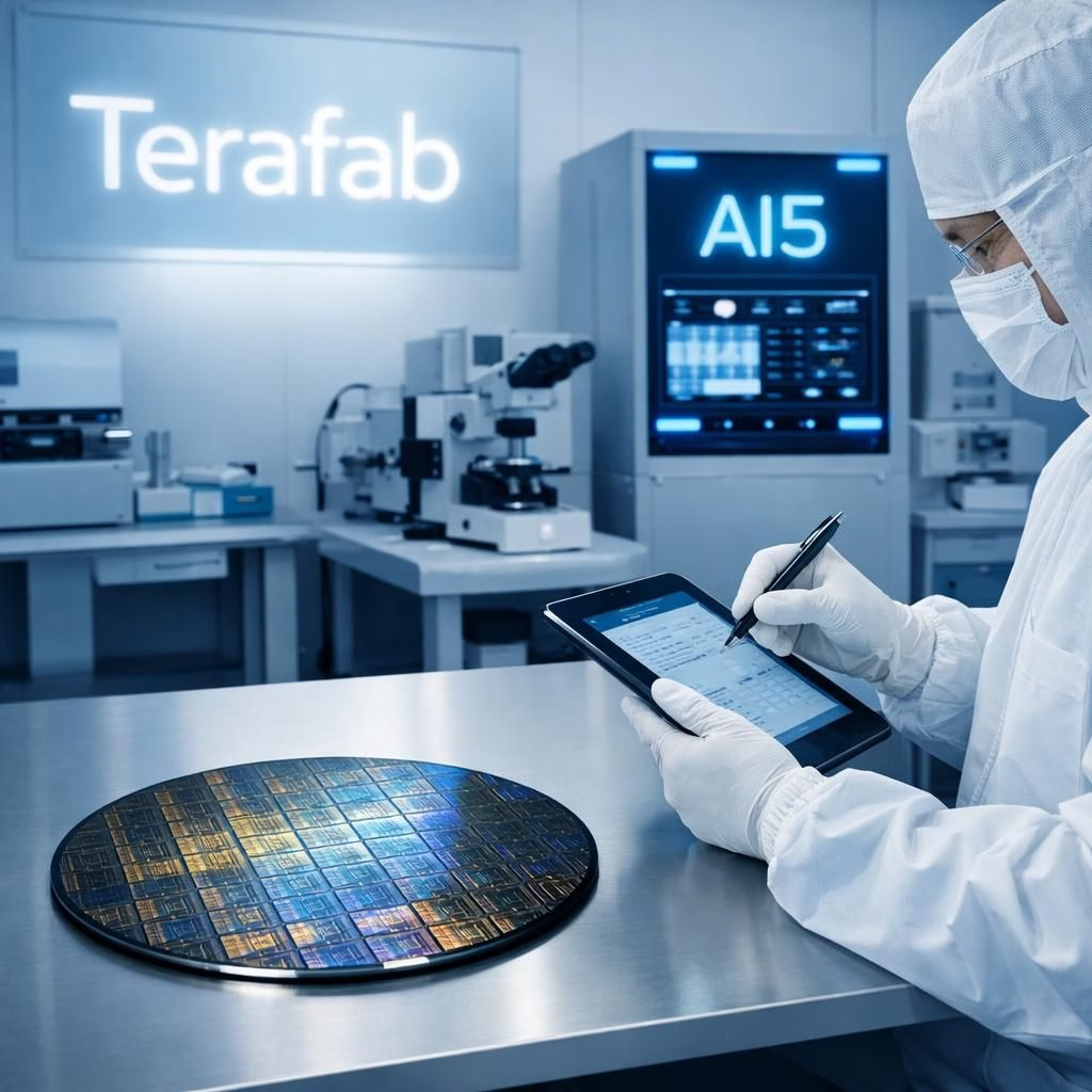
Terafab and AI5 step into the spotlight as Intel teams with Elon Musk’s sprawling consortium—SpaceX, Tesla, and xAI—to rewire silicon fabrication. The aim isn’t just to tinker but to refactor the entire silicon pipeline, from design through packaging. The audacious target is delivering 1 TW of compute per year for AI and robotics. If this were a movie, you would hear a narrator say that we are scaling silicon to star power.
Intel describes the partnership as a practical collaboration. The company brings its deep know-how in chip design, fabrication, and advanced packaging to the project, while Musk’s team provides vision, scale, and a healthy dose of can-do bravado. AI5 has already been described as the brain behind Tesla’s future platforms, and the materials emphasize refactoring silicon fab technology as a strategic pivot. The message is clear: a more integrated silicon life cycle could redraw timelines and budgets in meaningful ways.
Terafab: Refactoring silicon at scale
Terafab is framed as a joint venture with the ambition to harmonize design, fabrication, and packaging under one roof. In practice, that means new modular fabs, smarter process control, and a shift toward flexible lithography and packaging architectures that cut latency and boost yield. The goal of 1 TW/year would rely on far more than bigger ovens and shinier tools; it would require a unified platform for design automation, manufacturing software, and real-time feedback across multiple sites. Executives describe Terafab as a structural rethink rather than a cosmetic upgrade. If you imagine silicon as Lego bricks, Terafab aims to supply bricks with better connectors, clearer instructions, and a more forgiving glue—so you can assemble faster, test quicker, and scale with fewer surprises. In this frame, Terafab becomes the backbone for future AI accelerators and robotics chips, enabling rapid prototyping and robust production at scale.
Looking ahead, Terafab’s approach imagines a factory ecosystem where design and production decisions travel together, guided by data-driven feedback and standardized interfaces. Such a platform could reduce bottlenecks, shorten cycle times, and improve yields across the supply chain. The emphasis is on resilience as much as on performance, ensuring that a single disruption does not derail a whole run. Terafab’s architecture is intended to support the growing demand for AI-ready chips while keeping costs under control.
AI5 power and the Terafab vision
AI5 is presented not merely as another chip but as the brain at the center of Tesla’s most ambitious systems. Musk has framed AI5 as designed to be the core intelligence behind next-gen vehicles and robotics, while Terafab provides the manufacturing muscle to push volume and reliability. The collaboration envisions a future where AI5 chips flow through a refined supply chain that reduces cycle times from design to wafer, testing, and packaging. The emphasis is on energy efficiency, compute density, and interconnect reliability—qualities that could translate into swifter inference and more capable autonomous systems. The partnership’s rhetoric has a dash of bravura, but the underlying claim is practical: better silicon at scale can accelerate AI research, lower edge latency, and deliver more capable robotics platforms. AI5’s role here is to accelerate learning and inference across the Terafab ecosystem, enabling smarter decisions in data centers and on the factory floor alike.
Industry watchers may poke at the project with skepticism, but the leadership framing stays upbeat. The plan includes structured milestones, cross-company testing, and shared reference platforms designed to minimize surprises when the first AI5 chips roll off the Terafab line. The ambition of 1 TW/year remains a bold target—one that invites critique and ambition in equal measure. The practical takeaway is simple: if Terafab and AI5 can align design rules, fabrication steps, and packaging standards, the entire silicon supply chain could become more predictable, more adaptable, and more resilient in the face of demand shocks or geopolitical headwinds.
The product vision for Terafab emphasizes faster iteration cycles for AI accelerators and robotics chips. It aims to shorten the distance between architectural breakthroughs and real-world deployments in vehicles, factories, and data centers. Beyond the technical promise, the collaboration hints at a broader industry trend: a more integrated silicon life cycle from concept to production. If Terafab succeeds, researchers and manufacturers gain a more predictable supply chain that reduces vendor lock-in and improves coordination across design, fabrication, and packaging. The AI5 component remains central, aligning with Musk’s hardware strategy while inviting Intel to contribute its manufacturing discipline to a shared objective.
As with any large-scale venture, questions around cost, timelines, and the practical limits of refactoring will surface. Yet a core takeaway remains: Terafab envisions a new way to think about silicon. The target of 1 TW/year signals more than power; it suggests a harmonized workflow where design, fabrication, and packaging operate as a tightly choreographed system. If kept disciplined, this model could push the envelope on what hardware teams can achieve in a few years, influencing the CPU-GPU landscape and beyond.
Readers who enjoy a good engineering tale with a touch of aspirational humor will appreciate the spirit here: bold goals paired with serious engineering culture. The collaboration quietly signals a shift in how the tech industry might approach large-scale manufacturing—toward a holistic platform rather than a patchwork of point solutions. Terafab becomes the thesis, AI5 the argument, and their partnership the evidence that big players can co-create a credible path to modern silicon that benefits developers, researchers, and end users alike.
We invite you to share your thoughts in the comments below.
Practical implications and milestones
- Terafab aims to unify design, fabrication, and packaging into a single ecosystem, potentially reducing cycle times.
- A modular fab architecture and digital twin tooling could improve yields and allow faster deployment of AI-ready chips.
- Cross-company testing and shared reference platforms are planned to minimize surprises as AI5 chips move toward production.
FAQ
What is Terafab?
Terafab is a joint venture that aims to refactor silicon fabrication by unifying design, fabrication, and packaging under one roof, supported by SpaceX, Tesla, and xAI with Intel’s manufacturing expertise.
What does 1 TW/year of compute mean?
1 terawatt of compute per year is a capacity benchmark for AI and robotics workloads, reflecting aggregated processing across data centers and edge devices over a year.
How does AI5 fit into Terafab?
AI5 is designed to be the central AI brain for the system, with Terafab providing the scaling manufacturing capability to push AI5 chips into volume production.
When could a Terafab-enabled supply chain begin delivering chips?
Timelines remain uncertain; the project frames milestones, but external factors like supply chain shocks, policy, and funding will influence timing.
Conclusion
Terafab and AI5 embody a bold approach to modern silicon, combining Intel’s manufacturing discipline with Musk’s ambitious hardware program. If the plan stays disciplined, Terafab could help accelerate AI and robotics development by delivering more predictable, higher-quality silicon at scale. The collaboration signals a broader trend toward integrated silicon life cycles and platform-based hardware development.
References
External sources
- IEEE Spectrum: Semiconductors and AI hardware
- MIT Technology Review: AI hardware and computing trends
- Brookings: Global semiconductor supply chain risks